
China’s Diamond Revolution: How Lab-Grown Diamonds Could Transform Computer Chips
Key Takeaways
Lab-grown diamond has properties that interest chip researchers, but production scale alone does not make it ready for semiconductor use. Its near-term prospects may be more practical in heat management than in replacing silicon as an active chip material.
- Diamond can conduct heat effectively while remaining electrically insulating, a combination that could help manage chip temperatures.
- Industrial diamond production and semiconductor-grade material are not interchangeable: electronics need carefully controlled purity, crystal quality, and consistency.
- China’s large synthetic-diamond manufacturing base could matter to supply chains, but its scale does not by itself establish leadership in advanced chip components.
- Heat spreaders and other thermal-management uses appear closer to practical adoption than diamond transistors or other active devices.
- Commercial prospects will depend on measurable system-level gains, reliable integration, and costs that make sense to chipmakers.
Why diamond is attracting attention in semiconductor research
Diamond is drawing research interest because it combines several properties that are unusual in one material. The prospect is not simply to replace silicon, but to use diamond where its specific traits could address a design constraint. That distinction matters: a material can be excellent at moving heat and still be difficult to manufacture into a dependable electronic component.
How diamond’s thermal conductivity could help manage chip heat
As processors and accelerators perform more work in compact spaces, removing heat becomes a design challenge as well as a packaging one. Diamond can conduct heat efficiently, so researchers are exploring whether it could carry heat away from hot regions of a device or spread it across a larger area. The potential value is more effective heat movement, not a promise that a diamond layer will automatically make a chip faster or more energy-efficient.
A heat spreader also has to make good contact with the heat-producing component. If the interfaces between materials impede heat flow, the benefit of the diamond itself can be reduced. So the material is one part of a thermal path that includes the chip, attachment layers, package, and cooling system.
What its electrical properties offer beyond cooling
Diamond is an electrical insulator in many forms, but carefully engineered diamond can also be investigated as a semiconductor. Its wide bandgap and capacity to tolerate demanding conditions make it a candidate for certain high-power or high-frequency devices. Those possibilities depend on controlling impurities and defects so that the material behaves as intended.
This creates two distinct research tracks. In one, diamond helps manage heat without carrying the device’s electrical signal. In the other, it is part of the active device itself, where electrical behavior, contacts, and manufacturing tolerances all have to be engineered together.
How diamond compares with silicon, silicon carbide, and gallium nitride
Each material addresses a different mix of electrical, thermal, and manufacturing needs. A simple comparison is useful, but it should not be read as a ranking: the right choice depends on the device and the role the material is meant to play.
| Material | Common role in electronics | Potential strength | Key consideration |
|---|---|---|---|
| Silicon | Mainstream logic and many other chips | Mature, widely established manufacturing | Heat and performance limits depend on device design |
| Silicon carbide | Power electronics | Suited to demanding power applications | Processing and cost remain important factors |
| Gallium nitride | Power and high-frequency electronics | Useful electrical properties for selected applications | Integration and manufacturing requirements vary |
| Diamond | Thermal management and research devices | Strong heat conduction; potential for demanding electronic uses | High-quality material and integration are challenging |
Diamond is therefore more likely to enter as a complementary material before it displaces established semiconductor platforms. Researchers also study other material supply questions, such as China’s reported work on high-purity silicon-28, but that is a separate materials pathway with different aims. Comparisons are most useful when they describe a defined application rather than imply that one material is best across the board.
Why “diamond chips” can mean several different technologies
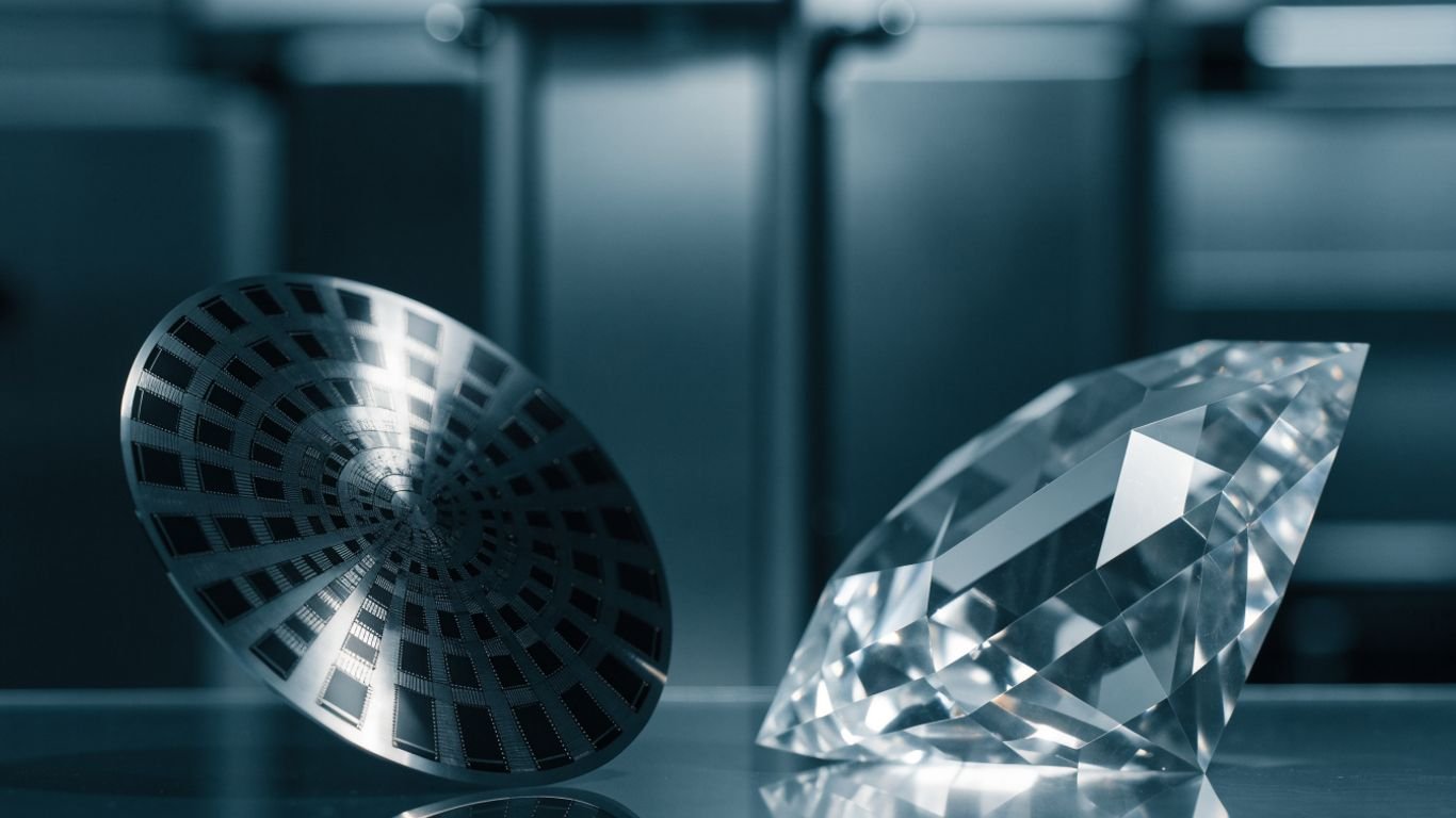
The phrase “diamond chips” can refer to very different ideas. It may mean a conventional chip attached to a diamond heat spreader, a diamond substrate supporting another semiconductor, or a device in which diamond itself performs an active electronic function. These approaches differ in technical maturity and in how much of the existing chipmaking process they would need to change.
The distinction helps keep ambitious claims in perspective. A thermal component can be valuable without being a transistor, and a laboratory demonstration of an active diamond device is not the same as a commercial processor built on diamond.
China’s role in synthetic diamond production
China’s established synthetic-diamond manufacturing base gives the country an important position in discussions about future material supply. But industrial output is only one part of the semiconductor question: chips require specific grades, consistent quality, and processing routes that fit demanding production standards. The distance between producing diamond in volume and supplying chip-ready components should not be glossed over.
How high-pressure, high-temperature and CVD methods create lab-grown diamond
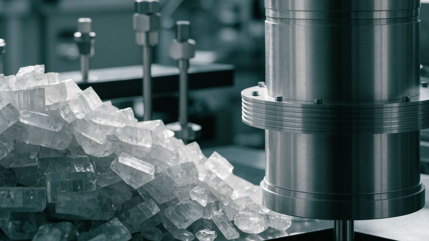
Two broad methods are used to make synthetic diamond. High-pressure, high-temperature (HPHT) production recreates conditions under which carbon forms diamond, while chemical vapor deposition (CVD) grows diamond from carbon-containing gas in a controlled environment. Each method can produce material for different uses, and the route alone does not determine whether a specimen is suitable for electronics.
The resulting crystals or films still need characterization and processing. Differences in defects, impurities, and uniformity can affect performance, so a description such as “lab-grown” says how the material originated, not whether it meets semiconductor requirements. A plain-language overview of synthetic diamond growth methods provides background on the basic processes.
Why China’s manufacturing base matters to the supply chain
A large production base can support equipment makers, specialized suppliers, and the accumulation of practical manufacturing experience. That may create advantages in cost or availability for some kinds of synthetic diamond. It does not guarantee that every producer can make electronic-grade material, or that buyers can use it without additional qualification.
Supply-chain significance also depends on what is being produced and where it is used. Industrial diamond can support cutting, grinding, or polishing, while semiconductor applications may demand precise characteristics and repeatability. Recent attention to China’s industrial diamond supply reflects this broader supply-chain interest, but the implications for chip components depend on the grade and application at issue.
The broader manufacturing picture is varied. Country Brief’s coverage also ranges across digital tools and physical goods, including Microsoft Fabric, BMW Vision Driving Experience, Cambria countertops, Bridge Bagels, and a WordPress help chat plugin. Those subjects are not evidence about diamond production; they illustrate how global business reporting spans very different supply chains and product requirements.
How industrial diamond production differs from semiconductor-grade material
Industrial diamond is often valued for hardness and durability in tools and machining. Semiconductor-related uses place different demands on the material: crystal structure, impurity levels, dimensions, and consistency can all matter. A producer that serves industrial markets may have relevant equipment and expertise, but that does not mean its output is automatically ready for a chip application.
The distinction is important when interpreting claims about national production capacity. Aggregate volumes can conceal differences between abrasive grades, gemstone material, heat-management components, and material intended for electronic devices. Assessing the supply chain requires asking what kind of diamond is being made, to what specification, and at what scale.
What researchers and companies are developing for chip applications
Research and commercial interest spans thermal components, substrates, and active electronic devices. These categories should be tracked separately because progress in one does not establish progress in the others. A heat spreader can use diamond without turning the underlying processor into a diamond semiconductor.
Chinese producers are also looking beyond traditional uses as they consider higher-value applications. Reports on diamond makers targeting technology markets describe that shift as an industrial ambition, not proof that semiconductor-grade products are already widely adopted. The next useful evidence will be repeatable component performance and customer qualification, rather than announcements alone.
Where diamond could fit into computer chips
Diamond’s most plausible roles depend on the problem a chip designer needs to solve. Some uses would add a diamond component to familiar architectures; others would require a more fundamental change to device materials and fabrication. That difference shapes both the engineering challenge and the likely time horizon.
Using diamond as a heat spreader for processors and AI accelerators
A diamond heat spreader could sit near a processor or accelerator and help move heat away from localized hot spots. This is attractive where high power density makes temperature management difficult, including in some data-center systems. Whether it improves a complete system depends on the package design and on the thermal path beyond the diamond layer.
The component would not eliminate the need for conventional cooling. Instead, it could be tested as one part of a package, with performance measured under realistic operating conditions. The relevant question is whether the whole assembly can sustain useful operation more effectively, not whether diamond has impressive material properties in isolation.
Exploring diamond substrates for power and high-frequency electronics
A substrate provides a base on which other device layers can be formed or mounted. Diamond’s thermal behavior makes it interesting as a possible support for power and high-frequency electronics, where heat and electrical performance can be closely linked. A substrate approach may also combine diamond with another semiconductor rather than asking diamond to do every job.
That combination brings its own constraints. The materials must be joined in ways that preserve performance, and the substrate must be manufacturable in suitable dimensions and quality. Early demonstrations can clarify what is physically possible, but practical adoption requires repeatability and compatibility with device production.
Integrating diamond with existing silicon devices
For many applications, integration may be more realistic than wholesale replacement. A diamond layer or component could be added to a silicon-based device or package while much of the established design remains intact. This route is still technically demanding, but it avoids assuming that the entire semiconductor ecosystem will switch materials at once.
The integration challenge includes bonding, surface preparation, thermal interfaces, and the sequence of manufacturing steps. A successful material coupon is only a starting point; the component must survive assembly and operate alongside other materials without introducing new failure points.
Investigating diamond as an active semiconductor material
An active diamond device would use diamond to control or carry electrical behavior, not merely to move heat. Researchers are interested in the possibility of devices suited to demanding environments, but crystal quality and controlled electrical properties remain central obstacles. Contacts and manufacturing methods also need to work reliably at useful scales.
This is a longer-term prospect than using diamond as a passive thermal component. It calls for advances across materials growth, device design, and fabrication, followed by evidence that the resulting devices can be produced consistently. Demonstrations are worth watching, but they should not be confused with commercial readiness.
What it takes to turn lab-grown diamond into chip components
A material’s promise only becomes useful when it can be made into a component that performs consistently inside a device. For diamond, that means controlling the material itself and solving the practical issues of cutting, shaping, joining, and testing it. The path from lab-grown crystal to chip component is a manufacturing challenge, not just a question of discovery.
Controlling crystal defects, impurities, and uniformity
Defects and impurities can alter how a crystal conducts heat or behaves electrically. Some applications may tolerate more variation than others, but semiconductor production generally depends on properties that are predictable from one batch to the next. Researchers therefore need ways to measure material quality and identify which characteristics matter most for a given use.
Uniformity also matters across a component, not only in a small sample. If properties vary across a film or crystal, performance may vary too. Better characterization can help set practical specifications, though it does not remove the challenge of producing material that meets them repeatedly.
Producing wafers and films with suitable size and quality
A useful component must be available in dimensions that fit its intended device. Producing diamond in small samples does not establish that larger wafers or films can be made economically and consistently. Size, thickness, surface condition, and yield all shape whether a research result can translate into manufacturing.
The requirements differ with the application. A small thermal element may face a different set of constraints from a substrate intended to support multiple device layers. Scaling up needs to preserve the relevant material properties, rather than simply increase the amount of diamond produced.
Connecting diamond to metals and other semiconductor materials
A chip component rarely works alone. Diamond may need to connect thermally or electrically with metals, silicon, or another semiconductor, and those interfaces can become weak points. Surface preparation and bonding methods must create reliable contact without damaging the materials or adding excessive resistance to heat flow.
Several practical questions make up this interface problem:
- Does the joint move heat effectively across the boundary?
- Can the materials remain attached through repeated heating and cooling?
- Does the connection fit the geometry and tolerances of the package?
- Can the joining method be repeated at manufacturing scale?
These questions show why material performance cannot be evaluated in isolation. A diamond part with excellent intrinsic properties may still disappoint if its connections to the rest of the device are poor.
Adapting fabrication processes for reliable device integration
Existing chip fabrication lines are designed around established materials and process controls. Introducing diamond may require new steps for cutting, polishing, bonding, or inspection, and each added step can affect cost and yield. Manufacturers will need to understand how the material behaves through the complete production sequence.
Integration also requires process compatibility. A component that works in a laboratory setup may not tolerate the temperatures, pressures, chemicals, or handling used in a production environment. Carefully designed trials can reveal whether a new process is practical before manufacturers commit to wider changes.
The technical and commercial hurdles
The case for diamond depends on whether it solves a real problem better than a less costly or easier-to-integrate option. That is a demanding test in electronics, where even modest changes can affect design, production, and reliability. Strong material properties matter, but they are only one part of the commercial calculation.
Balancing performance gains against production costs
Diamond components may justify their cost if they deliver a meaningful improvement in a system that is constrained by heat or performance. But the relevant comparison includes material production, processing, integration, and quality control—not just the cost of raw diamond. A premium material is hard to adopt if its benefit is marginal or difficult to measure.
Manufacturers will also consider whether the improvement can be achieved through package redesign or other established approaches. The result is not a simple contest between materials; it is a choice among engineering options, each with different costs, risks, and limits.
Addressing thermal interfaces and packaging challenges
Heat must travel from the active device through several layers before it reaches a cooler or heat sink. Any poorly performing interface can limit the value of a highly conductive spreader. Packaging geometry, attachment materials, and long-term stability all affect the result.
Tests should therefore evaluate the assembled package under conditions resembling actual use. A material’s laboratory thermal measurements are useful, but they cannot by themselves show whether a complete processor or accelerator will operate better. This is where careful system-level comparison becomes essential.
Meeting chipmakers’ reliability and qualification requirements
Electronic components must withstand years of operation and a range of temperatures, power loads, and environmental conditions. Buyers typically need repeatable production and evidence that the component will remain stable over time. New materials face a high bar because introducing them can create unfamiliar failure modes.
Qualification takes time, and a promising trial does not necessarily lead to procurement. Manufacturers need dependable supply, consistent specifications, and a clear path for handling defects or changes in production. Those requirements can slow adoption even when a component performs well in an early test.
Separating near-term cooling uses from longer-term device ambitions
Thermal management and active diamond electronics are often discussed together, but their development paths differ. Passive heat-spreading components may fit into existing designs with a more limited change to the device. Active diamond semiconductors require controlled electrical properties and more extensive process development.
Keeping those tracks separate makes claims easier to assess. Near-term progress should be judged through tested components and package performance; longer-term device ambitions need evidence of repeatable electrical behavior and manufacturable structures. Both may advance, but not at the same pace.
What could shape China’s diamond semiconductor prospects
China’s prospects will depend on more than its ability to produce synthetic diamond in volume. The material must meet demanding specifications, connect with existing chip technologies, and offer a clear advantage to users. That makes the story a question of industrial capability and market evidence, not production scale alone.
Tracking progress from laboratory demonstrations to commercial products
A laboratory result can establish that an approach is possible, but commercial use requires repeatability, manufacturing yield, and qualification by potential customers. Reports should distinguish between research prototypes, pilot production, and components being bought for routine use. Each stage answers a different question about maturity.
Useful evidence includes published performance under realistic operating conditions, information on material consistency, and confirmation that products have moved beyond demonstrations. Announced targets can indicate ambition, but they are not substitutes for these milestones.
Assessing supply-chain competition and access to specialized equipment
Production capacity depends on facilities, skilled workers, process knowledge, and access to equipment. A country may have strength in one part of the chain and rely on other sources for specialized machinery or downstream processing. Mapping those dependencies is more informative than treating national output as a single measure of control.
Trade policy can also influence supply, particularly for industrial materials used in precision manufacturing. Yet the effect of any restriction depends on which grades and applications are involved, how quickly buyers can find alternatives, and whether substitute material meets the same requirements. The details matter more than the headline category.
Identifying chip sectors most likely to adopt diamond first
Applications with acute thermal constraints may have the clearest reason to evaluate diamond components. High-power or high-frequency electronics could also be candidates where a specific combination of properties outweighs the added integration work. These are potential areas of interest, not guarantees of adoption.
A first use is likely to be narrow and application-specific. Manufacturers can test a material in a component where the performance target is clear before deciding whether broader deployment makes sense. That practical route is more plausible than an immediate switch across the chip industry.
Watching for evidence of performance gains at system level
The final test is whether diamond improves the device or system that uses it. Researchers and buyers will want results that account for the full package, operating conditions, reliability, and cost. Without that context, a material-level advantage may not translate into a better product.
For China, a durable position in this field would require linking production scale with advanced quality control, integration expertise, and customer confidence. The decisive developments may be quiet milestones—consistent batches, qualified components, and repeat orders—rather than dramatic claims about a revolution.
Conclusion
Lab-grown diamond has a credible place in semiconductor research because its thermal and electrical properties open several avenues for investigation. The most immediate possibilities appear to be complementary uses such as heat spreading, while diamond-based active devices remain a longer-term challenge. China’s production base gives the country a meaningful starting point, but commercial influence will depend on semiconductor-grade quality, reliable integration, and demonstrated gains in complete systems.
Frequently Asked Questions
Why are researchers interested in diamond for computer chips?
Diamond combines strong heat conduction with electrical properties that can be useful in selected applications. Researchers are studying both thermal components and possible electronic devices, which are distinct uses.
Can diamond replace silicon in processors?
There is no basis for treating diamond as a near-term replacement for silicon in mainstream processors. Its more plausible roles may be as a complementary material, particularly in thermal management, while active diamond devices remain under development.
What is the difference between HPHT and CVD diamond?
HPHT uses high pressure and high temperature to form diamond, while CVD grows diamond from carbon-containing gas under controlled conditions. The suitability of the resulting material depends on its quality and intended use.
Does China produce semiconductor-grade synthetic diamond at scale?
China has a large synthetic-diamond manufacturing base, but industrial output does not automatically indicate that semiconductor-grade material is available at scale. Quality, consistency, and application-specific specifications all matter.
How might diamond help cool AI chips?
A diamond component could potentially spread heat away from a concentrated hot spot in a processor or accelerator. The complete package still needs effective interfaces and cooling, so system-level testing is necessary.
What makes diamond difficult to use in electronics?
Challenges include controlling defects and impurities, producing material in suitable sizes, forming reliable connections to other materials, and adapting fabrication processes. Costs and long-term reliability also affect adoption.
When could diamond-based chip components become common?
Timing depends on demonstrated performance, manufacturing consistency, qualification, and cost. Thermal-management components may be more accessible than active diamond devices, but adoption will depend on evidence from real applications.