
Huawei’s 3D Microchip Technology: How It Works and Why It Matters
Key Takeaways
This article examines the recent architectural and software innovations driving self-reliance in semiconductor fabrication. By focusing on vertical integration, these advancements signal a shift in global chip manufacturing strategies.
- Huawei’s 3D microchip design aims to bypass Western equipment restrictions.
- Peking University has developed custom EDA tools to support vertical chip stacking.
- The Tau scaling law replaces traditional physical etching limits with temporal signal efficiency.
- Strategic shifts in domestic supply chains are challenging the existing semiconductor monopoly.
- Long-term goals include replacing high-end foreign AI hardware with sovereign domestic alternatives.
The geopolitical necessity of technological autonomy
National sovereignty in the modern era rests on the ability to produce high-performance hardware internally. Global supply chain fragility has exposed the dangers of over-reliance on external partners who may suddenly change export terms based on policy shifts. Recognizing these vulnerabilities, nations are now prioritizing the creation of robust, domestic ecosystems for advanced computation.
Overcoming western semiconductor embargos
The imposition of stringent export controls has forced a reckoning in domestic industry. Rather than waiting for the lifting of restrictions, engineers have sought methods to achieve performance goals that were previously considered impossible without specialized equipment. By finding creative workarounds for access to ASML’s extreme ultraviolet lithography, researchers are essentially building a parallel pathway to high-end compute density.
The shift away from globalist supply chains
A move toward localized production is gaining momentum as countries realize that dependencies are liabilities. By shortening the distance between design, manufacturing, and assembly, these firms hope to insulate their internal development cycles from external shocks. This realignment is not merely an economic decision but a fundamental defense strategy to ensure thatcritical semiconductor manufacturing equipment remains accessible regardless of international tensions.
National security as the primary driver of innovation
When foreign supply channels are threatened, security concerns dictate the trajectory of technological development. The focus has moved toward maintaining a stable supply of high-end processing power for AI and infrastructure needs. This transition is essential for maintaining a competitive edge where Nvidia’s hardware once stood as the sole, albeit vulnerable, pillar of high-level AI training.
Understanding the fundamentals of LogicFolding
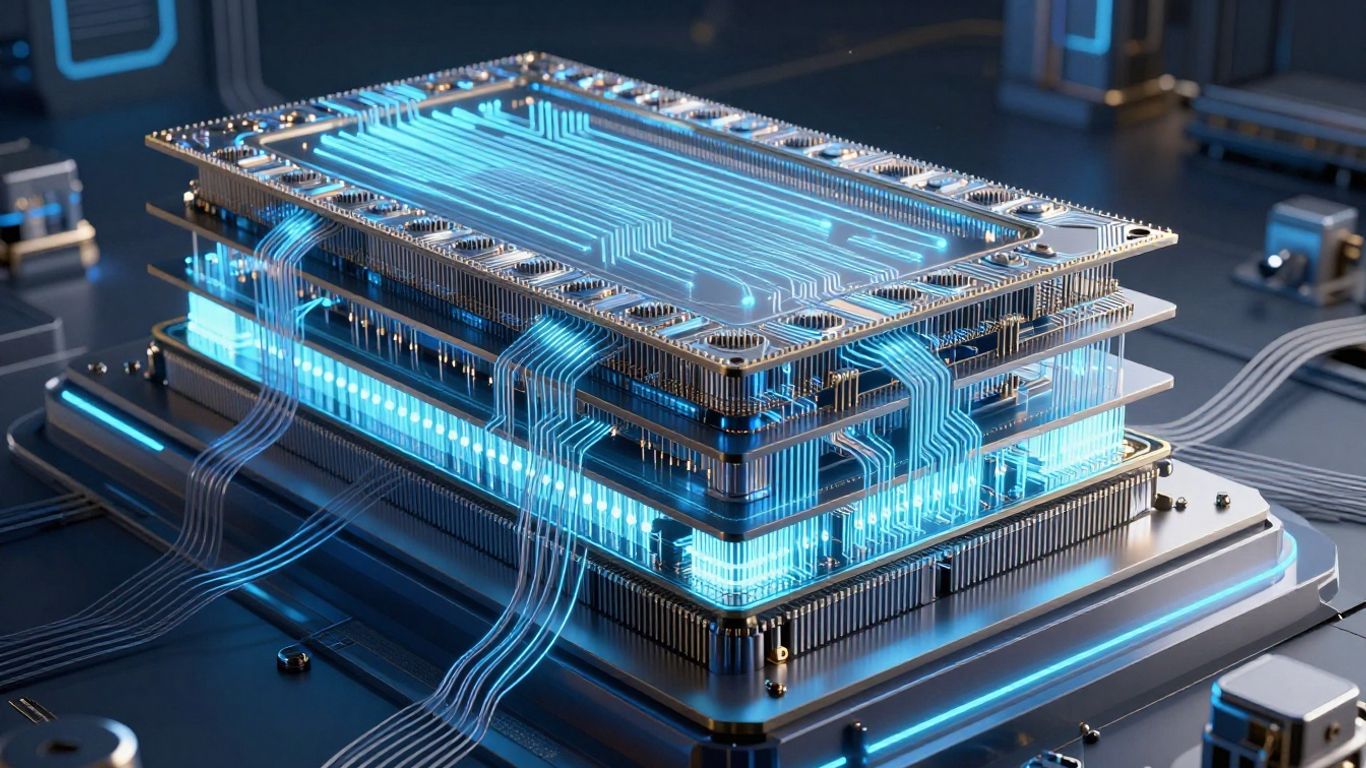
Huawei has introduced a new architectural paradigm known as LogicFolding, designed to increase transistor density without relying on traditional physical scaling methods. By treating the entire chip structure as a 3D volume instead of a flat set of dies, designers can optimize signal paths at the architectural level. This approach effectively circumvents the physical scaling limits imposed by restricted manufacturing nodes.
Moving beyond traditional 2D architecture
Traditional design has long been constrained by the limitations of flat silicon wafers. By moving to a 3D geometry, developers are creating a path to higher performance through better spatial organization. This shift allows for more efficient logic density, as engineers stop trying to force the laws of physics to accommodate smaller and smaller lithographic boundaries.
Improving transistor density without EUV lithography
The central hurdle for modern fabrication is the access to advanced etching machinery. Huawei’s 3D microchip approach addresses this by prioritizing spatial stacking instead of etching precision. By folding logical circuits, they can achieve performance equivalent to advanced nodes despite using less sophisticated fabrication techniques.
The advantages of vertical stacking in microprocessors
Vertical stacking allows for a significant reduction in signal propagation delay, as the physical distance between components is minimized. This architectural shift creates a faster, more efficient environment for data movement within the chip. It is a fundamental departure from legacy design that relies on increasingly complex flat layouts.
Developing domestic EDA software for chip resilience
Software capabilities are as vital as hardware manufacturing capacity in the current semiconducter race. Because design automation tools are dominated by established Western firms, the creation of unique, localized software has become a mission-critical requirement for the entire electronics sector.
The role of Peking University in custom design tools
Academic contributions have played a vital part in this shift, particularly in the creation of new placement and routing algorithms. Through the efforts of institutions like Peking University, designers now have access to native tools that are specifically optimized for local production methods. This collaborative effort between universities and industry giants helps bridge the gap left by international vendors.
Breaking dependence on western software providers
Standard software suites are built for ecosystems that ignore the needs of custom 3D hardware design. Transitioning to domestic software allows for greater flexibility in how chips are laid out. The table below compares common design tool strategies:
| Feature | Western Standard Tools | Custom Domestic EDA |
|---|---|---|
| Multi-die Scaling | Standardized | Native 3D Flow |
| Signal Delay Bias | Fixed | Tau Law Optimized |
| Hardware Linkage | Generic | Proprietary Hardware |
By prioritizing tools that handle unique layering, the industry reduces risks associated with software update restrictions or licensing lock-outs.
Custom software tailored to Huawei’s proprietary hardware
Custom design environments are being built to ensure maximum compatibility with unique stack configurations. These tools provide designers the freedom to optimize logic specifically for the electrical characteristics of vertically stacked chips, ensuring performance is not left on the table during the synthesis process.
Technical hurdles and breakthrough capabilities

Innovation brings significant engineering challenges, particularly regarding the physical constraints of stacked components. As layers are added, the complexity of managing the chip’s internal environment increases, demanding new solutions for existing structural limitations.
Managing thermal output and power distribution in 3D stacks
Heat management in compact, multilayer designs is a primary concern for any high-density processor. Advanced cooling solutions and power routing are required to ensure that the chip remains stable under high load. This engineering task is currently the main focus of ongoing research into efficient thermal dissipation paths.
Maintaining performance parity with legacy western alternatives
Achieving equality in raw power while lacking certain advanced materials or machines is a massive feat. Performance testing shows that the new architectural design can compete with legacy methods by leveraging logic density rather than sheer transistor smallness. This demonstrates that architectural intelligence can often compensate for mechanical limitations.
The iterative nature of scaling domestic chip fabrication
The move from laboratory concept to reliable mass production requires constant refinement. Engineers are currently iterating on test chips to find the balance between yield and performance. This iterative development is key to maturing the process before large-scale deployment across diverse consumer and enterprise products.
Implications for the global semiconductor arms race
Changes in fabrication philosophy are already influencing the global chip market. As traditional giants watch these developments, the monopoly on advanced computational hardware is starting to face significant pressure from new, divergent innovation paths.
Challenging the monopoly of the existing technological status quo
The reliance on a handful of manufacturing hubs has created a rigid global structure. Proactive development of domestic solutions serves as a direct challenge, forcing a reconsideration of how chip dominance is maintained globally. Several specific factors reflect this shifting landscape:
- Decreased reliance on high-cost imported lithography equipment.
- Faster product cycles due to localized software and design synergy.
- Shift of intellectual property value toward unique 3D architectural patents.
- Increased control over national digital privacy and infrastructure security.
This trend fundamentally threatens the traditional dominance of vendors who are heavily constrained by current global geopolitical alliances.
Competitive implications for major international chip innovators
Established players must now contend with a rival that is not trying to beat them at their own game but is changing the rules of the competition entirely. If 3D stacking proves viable at mass scale, the current focus on extreme etching precision may become less relevant for future development cycles.
Establishing sovereign technological power in East Asia
Regional cooperation is becoming more apparent as the need for a stable, self-contained circuit becomes clearer. By fostering a local environment where design, software, and fabrication interact seamlessly, the foundation is being laid for long-term technological independence.
Roadmap for future self-reliant semiconductor production
Looking beyond immediate milestones, the long-term objective is to normalize high-performance manufacturing without external reliance. The path ahead requires consistent focus on building out the entire ecosystem, from raw material processing to finished module assembly.
Moving from experimental design to mass-scale manufacturing
The industrialization of laboratory breakthroughs requires a shift in mindset toward reliability and cost-efficiency. This is the most difficult stage of the roadmap, as moving to a high-volume process exposes flaws that were not apparent in smaller, controlled production runs.
Prioritizing national investment in hardware engineering talent
Training the next generation of engineers is vital for sustaining this progress. Investment in technical education and infrastructure ensures a steady pipeline of domestic talent capable of managing the specialized demands of 3D chip architectures and their associated design tools.
Long-term impact on the global technology landscape
In the coming decade, we will likely see a bifurcation in architectural approaches between those wedded to traditional 2D scaling and those innovating through 3D logic folding. This shift will influence not just chip production, but everything from AI data centers to mobile processors, eventually restructuring the entire global technology market.
Conclusion
The transition toward vertically integrated, 3D logic architectures marks a decisive moment in technological sovereignty. By addressing the barriers created by export restrictions through native architectural ingenuity and home-grown software tools, the industry is paving a new route to high-end performance. As domestic fabrication capacity continues to mature, we are likely to witness a profound shift in influence, where internal resourcefulness becomes the most valued asset in the race for advanced computation power.
Frequently Asked Questions
What makes 3D chip architecture different from traditional 2D methods?
Traditional 2D chips are laid out on a flat surface, whereas 3D architecture stacks layers of circuitry on top of each other, allowing for greater density and shorter signal paths.
Why is domestic electronic design automation software important?
Domestic design software allows developers to create and test chips without depending on foreign vendors, ensuring that the development process remains immune to external political pressure.
How does LogicFolding increase transistor density without etch precision?
It achieves high density through structural efficiency rather than sheer miniaturization, using specialized layer stacking to optimize space usage within the chip’s physical footprint.
Is this technology currently available for commercial consumer devices?
Initial applications for these advanced architectures are being integrated into new generations of smartphone processors, with more widespread deployment across diverse hardware expected in the near future.
What are the main thermal difficulties of vertical chip designs?
Heat dissipation is a challenge because vertical stacks limit airflow and create internal regions that are difficult to cool, requiring advanced material and design strategies to move heat away from the core.
Can 3D scaling really replace geometric etching refinement?
While it does not perfectly replicate every physical benefit of etching, it provides an alternative pathway to achieve similar performance metrics by maximizing the utility of the available vertical space.
What is the long-term goal of adopting these internal scaling laws?
The goal is to build a self-sufficient industrial base capable of producing high-performance compute hardware to support national AI and digital infrastructure goals without relying on foreign entities.